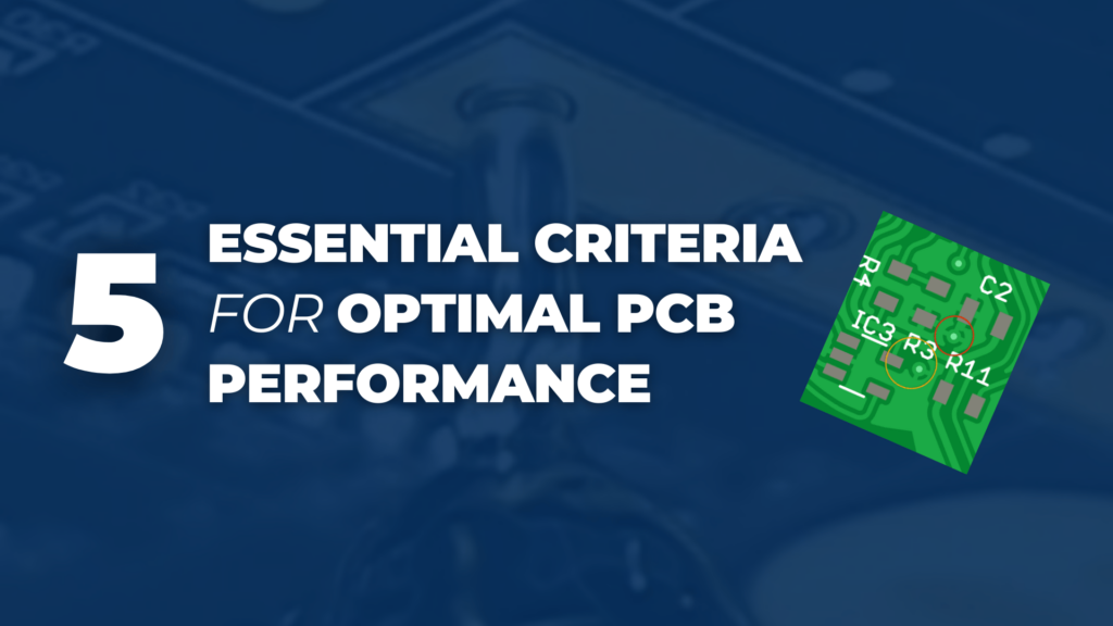
Mastering Selective Soldering: 5 Essential Criteria for Optimal PCB Performance
April 8, 2025
Table of contents
Selective soldering is a critical process in electronics manufacturing that allows precise soldering of through-hole components while minimizing exposure to other areas of a printed circuit board (PCB). To gain insights into best practices for optimizing PCBs for selective soldering, we spoke with Maksym Riazantsev and Andriy Pankiv, who are seasoned professionals in electronic manufacturing with years of hands-on experience in process optimization and soldering technologies at TECHTO Electronics.
In this interview, they pinpointed 5 key criteria for ensuring effective selective soldering, the potential challenges, and solutions manufacturers can implement to improve efficiency and reliability.
What are the key Criteria for Selective Soldering?
Maksym Riazantsev: I can think of a few that we have been applying on different PCBs for diverse products. Spacing around the component is one. The limitations about component height are another one.
Andriy Pankiv – The PCB label placement, solder bridging, and of course the heat tolerance of component materials easily come to mind.
Q: What are the spacing considerations for through-hole (THD) components in selective soldering?
Maksym Riazantsev: The spacing around through-hole (THD) components is one of the most important considerations in selective soldering. Ideally, the spacing should be at least 5mm in diameter from the nearest component to allow the soldering machine to operate without advanced programming. However, when space is limited, manufacturers can use small-diameter nozzles that provide a more controlled solder spot size. These nozzles allow soldering closer to surface-mount technology (SMT) devices and within metalized areas. To ensure consistent results, fine-tuning parameters and conducting test runs on spare PCBs are necessary before reducing production spacing.

Q: How does component height impact the selective soldering process?
Maksym Riazantsev: This component height issue is another crucial factor. If components exceed 14mm in height, such as coils, transformers, and capacitors, they can interfere with the nozzle movement. The standard nozzle size from manufacturers like Kurtz Ersa is 2mm inner diameter and 4.5mm outer diameter, meaning taller components may require special tooling, which can increase costs. Proper design planning can help minimize these issues and ensure smooth soldering operations.

Q: What issues arise from poor PCB label placement?
Andriy Pankiv: PCB label placement must be optimized to avoid direct exposure to hot solder. Labels positioned in areas exposed to hot solder can lead to detachment due to the glue melting. Although labels can survive brief contact with heat, their shape and legibility may degrade. In any case, the labels should be placed in areas not directly exposed to soldering heat. If that cannot be avoided, one should consider laser marking PCBs.

Q: What factors contribute to solder bridging, and how can it be minimized?
Andriy Pankiv: Solder bridging is another challenge in selective soldering. Factors such as long lead lengths, large pad sizes, and narrow pin pitch contribute to bridging. To minimize this risk, manufacturers should optimize soldering parameters, including temperature, flux quantity, and dwell time. Increasing the distance between component leads and ensuring proper flux application can significantly reduce the occurrence of solder bridges. In cases where bridging occurs, manual rework may be necessary.

Q: How does material selection impact selective soldering?
Andriy Pankiv: The heat tolerance of component materials is a final key consideration. Some components, particularly low-cost connectors, may melt due to prolonged soldering times. This typically happens when a pin is connected to a power plane, acting as a large heat sink. Implementing thermal reliefs in PCB layouts can help distribute heat more effectively, preventing excessive soldering times. Additionally, using high-quality, heat-resistant connectors reduces the risk of component damage. If certain pins remain problematic, they can be excluded from the selective soldering program and soldered manually.

Any concluding remarks?
Andriy Pankiv: Designing PCBs for selective soldering requires these practices because they help manufacturers enhance yield rates. They reduce defects and at the same time improve overall soldering efficiency.
Maksym Riazantsev: Designers should seriously consider collaborating with manufacturing engineers early in the process. In doing so, they can avoid costly design revisions and also optimize production workflows. This will reduce the cost of production, as the manual production time will be reduced accordingly.
Maksym Riazantsev is the Production Manager at TECHTO Electronics. In addition to overseeing production planning and control, he focuses on process optimization and automation to enhance efficiency and productivity.
Andriy Pankiv is the Chief Mechanic at TECHTO Electronics. He ensures the optimal condition of existing equipment and selects and integrates modern machinery to meet various production needs.
TECHTO Electronics is a leading Electronic Manufacturing Services (EMS) provider with state-of-the-art facilities in Ukraine and Denmark. Leveraging advanced manufacturing processes with an agile approach, TECHTO delivers high-quality electronic assemblies and components with European quality at Far East prices.