EMC Debugging: A Guide to Resolving EMI Challenges
December 11, 2024
Table of contents
Electromagnetic Compatibility (EMC) problems often disrupt electronics design and production. They cause device failures, missed regulatory standards, and costly delays. Diagnosing and fixing these issues can be frustrating, leaving teams scrambling for solutions. But with the right approach, you can identify the root causes and apply effective fixes.
This guide explains how to tackle EMC problems effectively. We will walk you through common challenges, essential tools, and best practices for resolving EMI issues and ensuring your devices perform reliably.
What is EMC Debugging?
EMC debugging is the process of finding and fixing problems with electromagnetic interference (EMI) or susceptibility that prevent devices from meeting EMC standards. These issues can come from poor design, faulty parts, or external factors. Effective debugging ensures devices work properly in their electromagnetic environment.
Common EMC Challenges in Electronics Design
Electromagnetic Compatibility (EMC) issues often arise during the design and production of electronic devices. Understanding these challenges is essential for building systems that operate reliably and comply with regulations.
Here are the three most common EMC challenges, and their causes and impacts.
1. Radiated Emissions
Radiated emissions occur when a device unintentionally emits electromagnetic energy into its surroundings. This energy can interfere with nearby equipment, disrupting operations or causing failures. Some design flaws that often lead to radiated emissions are
- Improper PCB layout: Poorly routed traces or large loop areas can act as unintended antennas, radiating unwanted signals.
- Poor grounding practices: Ineffective grounding can allow noise to escape from the device.
- Unshielded cables or components: Without adequate shielding, cables and components can emit electromagnetic energy into the environment.
2. Conducted Emissions
Conducted emissions refer to noise that travels along power or signal lines, affecting other devices connected to the same network or system. This is particularly problematic in environments with sensitive or interconnected equipment. Common causes include:
- Switching Power Supplies: These often generate high-frequency noise, which can travel through power lines.
- Insufficient Filtering: Without adequate filters, noise escapes the device and spreads through connected lines.
- Ineffective Cable Management: Poorly routed or improperly shielded cables can act as conduits for conducted noise.
3. Susceptibility Issues
Susceptibility occurs when a device cannot resist electromagnetic fields from external sources, leading to erratic behavior, data loss, or even device resets. This makes the system unreliable. Key contributors to these issues are:
- Inadequate Shielding: Devices without proper shielding are vulnerable to external electromagnetic fields.
- Improper Grounding: Weak grounding increases susceptibility to interference.
- Lack of Input Filtering: Without filters, external noise can enter through power or signal lines, disrupting device performance.
By identifying and addressing these challenges, designers can create more robust electronic systems that operate reliably in real-world conditions. The following sections cover tools and strategies to overcome these EMC problems.
Key Steps in EMC Debugging
Effective EMC debugging follows a clear, systematic process. Here are the steps:
1. Define the Problem
Start by identifying the specific EMC challenge. Review test reports to pinpoint failure points and frequencies. Focus on whether the problem involves excessive emissions, susceptibility to external interference, or both.
2. Localize the Issue
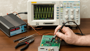
Find the source of the issue. Use tools like near-field probes, spectrum analyzers, and oscilloscopes to track emissions or measure areas where the device is most susceptible. This step helps you focus on the root cause.
3. Apply Design Fixes
Once the problem is identified, apply targeted solutions. Typical fixes include:
- Optimizing PCB layouts to minimize loop areas to reduce emissions.
- Ensuring the grounding system is robust and well-implemented.
- Utilizing appropriate shielding materials and installing filters to block or reduce unwanted noise.
Following these steps helps resolve EMC problems efficiently and improves device performance.
Essential Tools for EMC Debugging
Solving EMC problems requires the right tools. These tools help engineers identify, measure, and address electromagnetic interference effectively.
1. Spectrum Analyzers
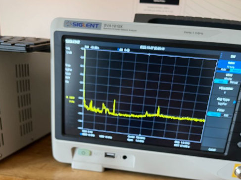
Spectrum analyzers detect and display emission frequencies across the electromagnetic spectrum. They allow engineers to pinpoint problem frequencies and assess their severity. This information is key to understanding how emissions interact with other systems.
2. Near-Field Probes
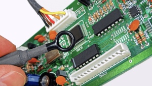
Near-field probes measure electromagnetic fields near specific components or areas of a circuit. These tools help locate high-emission points on a PCB, making it easier to target the root cause of a problem.
3. Oscilloscopes
Oscilloscopes display signals over time, making them useful for analyzing how circuit behavior relates to EMC issues. By observing time-domain signals, engineers can connect spikes or irregularities to specific events or components.
4. EMI Chambers
EMI chambers create a controlled testing environment free from external electromagnetic interference. They allow for accurate measurement and debugging of emissions and susceptibility without outside noise affecting the results.
Using these tools together ensures a thorough and efficient approach to EMC debugging, reducing the time needed to identify and solve problems.
Best Practices for Preventing EMC Issues
Preventing EMC issues during the design phase saves time and resources compared to fixing problems later. The following practices can help ensure your device meets EMC standards and performs reliably.
1. Optimize PCB Design
Good PCB design reduces electromagnetic emissions and improves signal integrity.
- Minimize signal loops: Keep loop areas small to reduce unintended radiation.
- Use multi-layer PCBs: Include dedicated ground planes to maintain signal integrity and reduce noise.
- Avoid trace overlap: Keep power and signal traces separate to prevent unwanted coupling.
2. Implement Robust Grounding
Proper grounding is critical for controlling noise and reducing emissions.
- Design low-impedance ground systems: Use short, wide traces and ground planes to lower impedance.
- Single ground reference: Connect all components to a single, shared ground point.
- Avoid ground loops: Ensure the ground network does not form loops, which can pick up or emit interference.
3. Use Effective Shielding
Shielding blocks electromagnetic energy from entering or leaving the device.
- Metal enclosures: Use metal casings to contain radiated emissions.
- Continuous cable shielding: Ensure cable shields are uninterrupted and properly connected at both ends.
- Seal openings: Minimize gaps in enclosures to maintain the shield’s effectiveness.
4. Incorporate Filters
Filters suppress noise and block unwanted frequencies.
- Ferrite beads and common-mode chokes: Place these components on power and signal lines to limit high-frequency noise.
- Low-pass filters: Use these to block frequencies above the operational range.
- Decoupling capacitors: Install capacitors near power pins to stabilize voltage and filter noise.
Follow these practices, so you can design systems that are less prone to electromagnetic interference, improving performance and ensuring compliance with EMC standards.
Importance of Early EMC Considerations
Addressing EMC during the early stages of design is more effective than fixing issues later. Early planning saves time, reduces costs, and improves the overall reliability of the device.
- Simulate and model potential EMI sources: Use simulation tools to identify and address possible interference before building physical prototypes.
- Select EMC-friendly components: Choose components designed to minimize emissions and resist interference. This reduces the likelihood of problems later.
- Follow regulatory guidelines: Design with compliance standards in mind from the start to avoid costly redesigns or testing failures.
By integrating EMC considerations into the initial design, you can build systems that are robust, compliant, and ready for the real world.
Collaborating with EMC Experts
If internal efforts fall short, collaborating with EMC experts or certified test labs can provide the support needed to resolve complex issues. These professionals bring:
- Specialized knowledge: EMC experts have a deep understanding of electromagnetic interference and can identify root causes that may be missed during internal troubleshooting.
- Advanced equipment: Certified labs are equipped with tools like anechoic chambers, advanced spectrum analyzers, and precision probes, enabling thorough diagnosis and testing of EMC problems.
- Compliance Insights: EMC experts are up-to-date with the latest regulatory standards and can help you navigate compliance requirements efficiently.
Working with experienced professionals ensures faster resolution of EMC problems and helps prepare your design for testing and production.
Conclusion
EMC debugging is critical for ensuring electronic devices meet performance and compliance standards. By recognizing common challenges, using the right tools, and following best practices, you can streamline the debugging process and improve product reliability.
Addressing EMC problems early in design, applying sound engineering principles, and collaborating with experts can help minimize risks. This proactive approach ensures your devices are well-prepared to meet EMC standards and succeed in the market.


